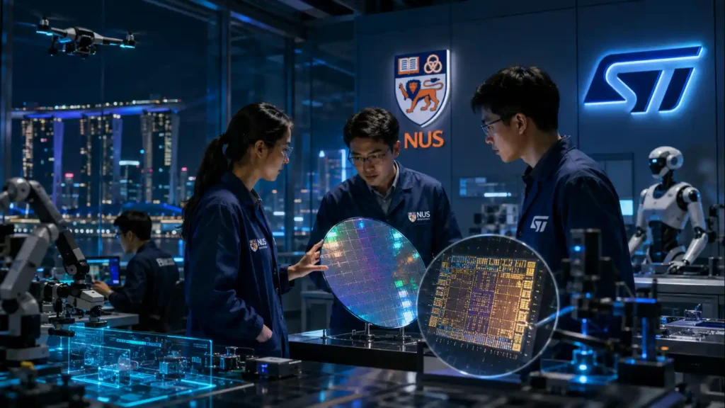
STMicroelectronics and the National University of Singapore (NUS) launched the ST–NUS HELIX Corporate Lab in Singapore on August 24, 2026. The four-year program will combine NUS research with ST’s 18nm FD-SOI and embedded phase-change memory platform to develop energy-efficient edge AI hardware for generative and embodied systems.
HELIX stands for Hardware for Embodied Low-power Intelligent Xcceleration. Supported under Singapore’s Research, Innovation and Enterprise 2025 plan, the lab is hosted by the NUS College of Design and Engineering with participation from the NUS School of Computing. Its scope runs from AI models and accelerators to memory hierarchies, circuit design, chip integration and silicon implementation.
The launch targets the hardware problem behind robots, humanoids, drones and other physical systems that must process sensor data and act in real time. It does not announce a finished processor. ST and NUS have not disclosed the lab’s budget, staffing, first prototype date, benchmark targets, licensing terms or commercialization schedule.
What Is the ST–NUS HELIX Corporate Lab Building?
HELIX is built around a system-to-silicon workflow rather than a single chip announcement. NUS and ST researchers will start with AI models and application needs, then work downward through system architecture, heterogeneous accelerators, on-chip memory hierarchies, circuit design, chip integration and silicon implementation. The shared platform is a dedicated design chassis in ST’s proprietary P18 18nm Fully Depleted Silicon On Insulator process. P18 supports adaptive body biasing, which lets designers tune a circuit’s speed and power behavior, while embedded phase-change memory adds non-volatile storage beside SRAM. That combination matters because repeatedly moving model weights and sensor data to external memory consumes energy and adds delay. Keeping more data and computation close together could help robots, drones and other constrained devices respond locally. The partners say joint work will also cover intellectual property, demonstrations and talent development, but they have not published project-level milestones or a tape-out schedule.
The official ST announcement says the company will give NUS a dedicated P18 design chassis. That matters because researchers can test accelerator concepts on an industrial platform instead of first creating the underlying process infrastructure. The NUS account of the launch confirms that joint work will include research packages, talent development, intellectual-property creation and demonstrations.
Why Does Memory-Centric Edge AI Matter?
Edge AI works within a different budget from cloud AI. A data-center model can draw on large accelerators, high-bandwidth memory and constant networking; a robot or sensor may have tight power, thermal, space and connectivity limits. HELIX therefore targets memory bandwidth, latency, energy efficiency, scalability and integration as one connected design problem. Its in-memory-computing research will explore performing some operations where data is stored, reducing transfers between memory and processing units. Its scalable compute-and-memory work can investigate how multiple blocks cooperate as workloads grow. For embodied AI, the practical test is not only model accuracy. Hardware must ingest multimodal sensor data, run inference within a real-time control loop and trigger safe physical action without depending on a distant server. Local processing can also limit how much raw data leaves the device. Those are intended research directions, however, not measured HELIX results; no prototype benchmark, power figure or latency result was announced at launch.
That focus connects the lab to two wider hardware trends. AI developers are trying to reduce memory movement, a constraint also driving the AI memory research race. At the same time, robotics companies need local perception and control before ambitious humanoid deployment plans can work reliably outside controlled demonstrations. Privacy-sensitive applications may also benefit when raw sensor data stays near the device, a relevant consideration for wearable biomarker AI.
How Does ST’s 18nm Platform Compare With Its Earlier Technology?
ST has published reference figures for the P18 technology underpinning the HELIX chassis. These are vendor comparisons against ST’s earlier 40nm embedded non-volatile-memory technology, not independent HELIX results.
The comparison figures come from ST’s P18 technology disclosure. The STM32V8 specifications come from a separate November 2025 product announcement. They show that HELIX is starting from a developed semiconductor platform, but they do not predict the speed, accuracy, efficiency or release date of any accelerator created by the lab.
How Could the Research Move From Lab to Device?
The program’s practical advantage is co-design. Researchers can begin with a real workload, determine where model execution is limited by memory or data movement, then adjust algorithms, accelerator blocks, memory hierarchy and circuits together. A promising design can be integrated into the P18 chassis, validated at system level and demonstrated in an embodied-AI use case. ST’s manufacturing and engineering teams can then assess whether the design is scalable.
The hard part will be proving that a concept remains accurate, reliable and energy-efficient after it leaves simulation. In-memory computing can reduce transfers, but designers still need to manage precision, memory behavior, software tooling, security and thermal limits. Robots and drones also add safety-critical timing: a good average latency is not enough if worst-case response breaks the control loop. HELIX has named these problem areas, but it has not disclosed target models, datasets, benchmark suites or test conditions.
Laurent Malier, ST’s executive vice president for Global Technology R&D, called the lab an “industrially relevant foundation” for “scalable semiconductor solutions.” Both statements appear in the NUS launch release.
Why Does the Corporate Lab Matter to Singapore and ST?
HELIX follows Singapore’s Corporate Laboratories model, which links public research institutions with companies around industry-directed R&D. The National Research Foundation’s program overview shows that the model is designed to combine academic research with industry mentorship and routes toward commercial prototypes. The HELIX release confirms RIE2025 support, but it does not state the program’s individual funding amount.
For Singapore, the lab adds hands-on training in AI systems, integrated circuits and advanced memory. For ST, it expands access to research talent while keeping projects close to an industrial design flow. ST is large enough to offer that route: its 2026 company snapshot lists 49,000 employees, 9,000 people in R&D and product design, 14 main manufacturing sites, operations in 40 countries and more than 200,000 customers.
What Has Not Been Announced?
Several details will decide whether HELIX produces useful technology rather than only research papers:
- The total budget and each partner’s financial contribution
- The number of researchers, students and engineers assigned to the lab
- The first silicon tape-out, prototype or public demonstration date
- Target AI models, workloads, accuracy thresholds and energy or latency benchmarks
- Publication, licensing and ownership rules for jointly created intellectual property
- A product roadmap or named commercial customer
The most meaningful next evidence would be measured silicon results under disclosed test conditions. Energy per inference, end-to-end latency, memory traffic, model accuracy and thermal behavior would make HELIX comparable with other edge AI platforms. Until then, the launch should be read as a serious research-and-infrastructure commitment, not proof of a new market-leading chip.
Official STMicroelectronics Contact Details
Readers looking for STMicroelectronics locations should use the company’s official contact directory. ST’s corporate legal seat is in Amsterdam, its head office is at WTC Schiphol Airport, and its operational headquarters are at 39 Chemin du Champ des Filles, 1228 Plan-les-Ouates, Geneva, Switzerland, with main telephone +41 22 929 2929, according to its 2026 semiannual report.
For this Singapore launch, the official release lists ST media contact Dennis Tan at +65 6216 5000 and [email protected]. ST’s investor-relations address and email are published on its investor contact page. These are corporate and media channels, not technical-support or lab-application contacts.
Key Takeaways
- STMicroelectronics and NUS launched HELIX as a four-year edge AI research program in Singapore, not as a finished chip or commercial product.
- The lab will co-design AI models, accelerators, memory systems and circuits on ST’s P18 18nm FD-SOI platform with embedded phase-change memory.
- ST’s published P18 gains are vendor comparisons with its earlier 40nm technology; HELIX has not released prototype benchmarks.
- Budget, staffing, tape-out dates, target models, IP terms and commercialization milestones remain undisclosed.
FAQ
Does Tesla use STMicroelectronics?
The HELIX announcement does not mention Tesla. ST says in its official company snapshot that it serves more than 200,000 customers, but its public materials do not provide a complete customer-by-customer list. A current direct Tesla–ST supply relationship therefore cannot be confirmed from the primary sources used for this article; product teardowns or older reports should not be treated as proof of an active contract.
Why is STMicroelectronics falling?
That question needs a market and date because STM trades in New York, Paris and Milan, and its price changes daily. Semiconductor shares can react to demand, margins, inventories, capital spending, currencies and guidance. ST’s Q2 2026 results do not by themselves describe a broad deterioration: revenue was $3.49 billion, up 26% year over year, with a 34.8% gross margin, while Q3 revenue guidance was $3.70 billion at the midpoint. Investors should compare any specific decline with the filing or news released that day rather than attribute it to the HELIX lab.
Is STM a big company?
Yes. STMicroelectronics is a large global integrated device manufacturer. Its official company snapshot lists $11.8 billion in 2025 revenue, 49,000 employees, 9,000 people in R&D and product design, 14 main manufacturing sites, offices in 40 countries and more than 200,000 customers worldwide. STM is its New York Stock Exchange ticker.
Where is STMicroelectronics HQ?
According to the company’s investor FAQ, STMicroelectronics is organized under Dutch law, with its corporate legal seat in Amsterdam and head offices at WTC Schiphol Airport in the Netherlands. Its headquarters and operational offices are managed through STMicroelectronics International N.V. at 39 Chemin du Champ des Filles, 1228 Plan-les-Ouates, Geneva, Switzerland. The distinction explains why official sources may refer to either the Netherlands or Geneva.